
One of my friends from the local Amiga users group has a TF534 accelerator that one day decided to fail. This post documents my repair of it.
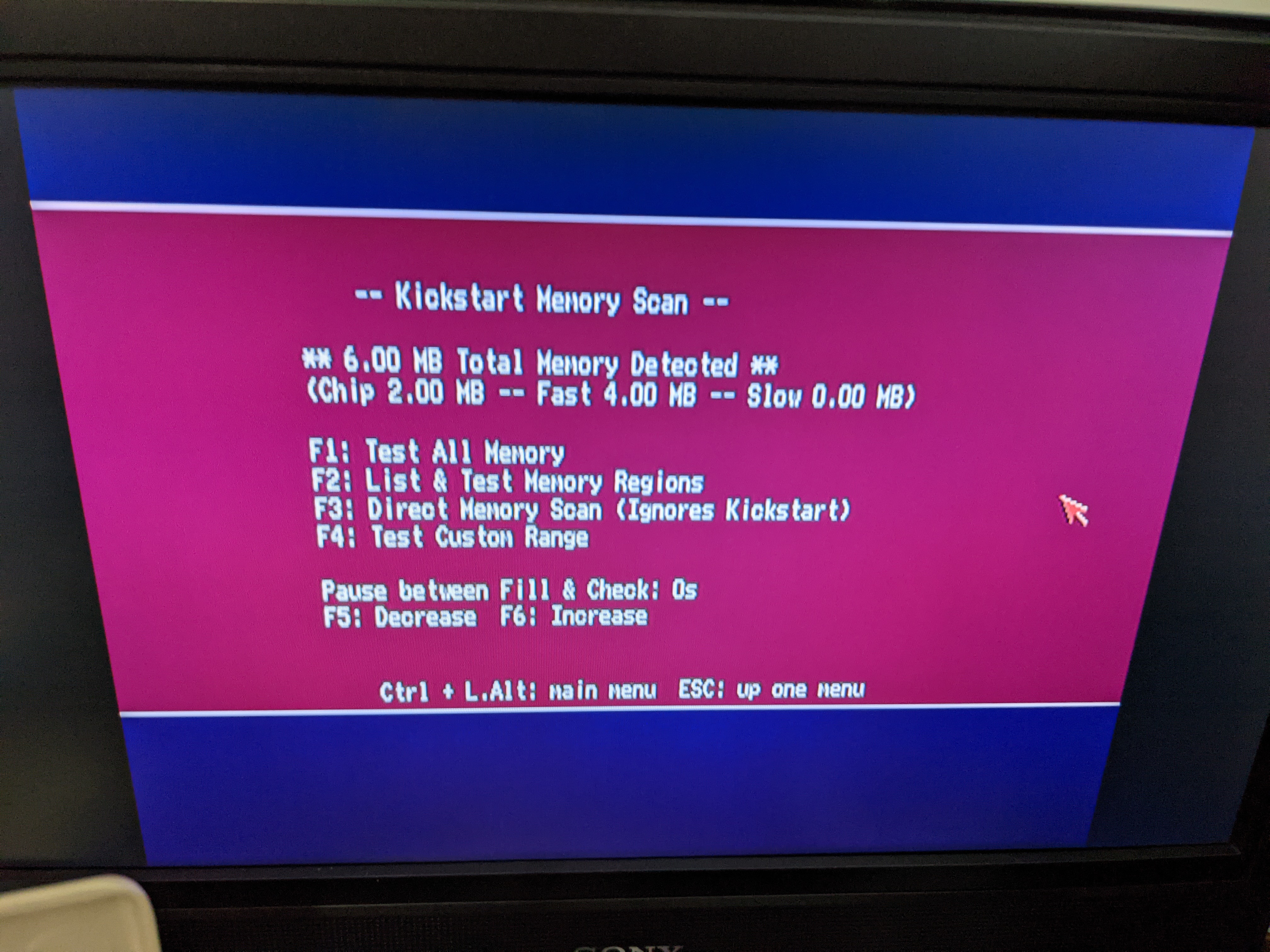
Upon booting his machine, the Kickstart ROM’s diagnostic started showing this screen.

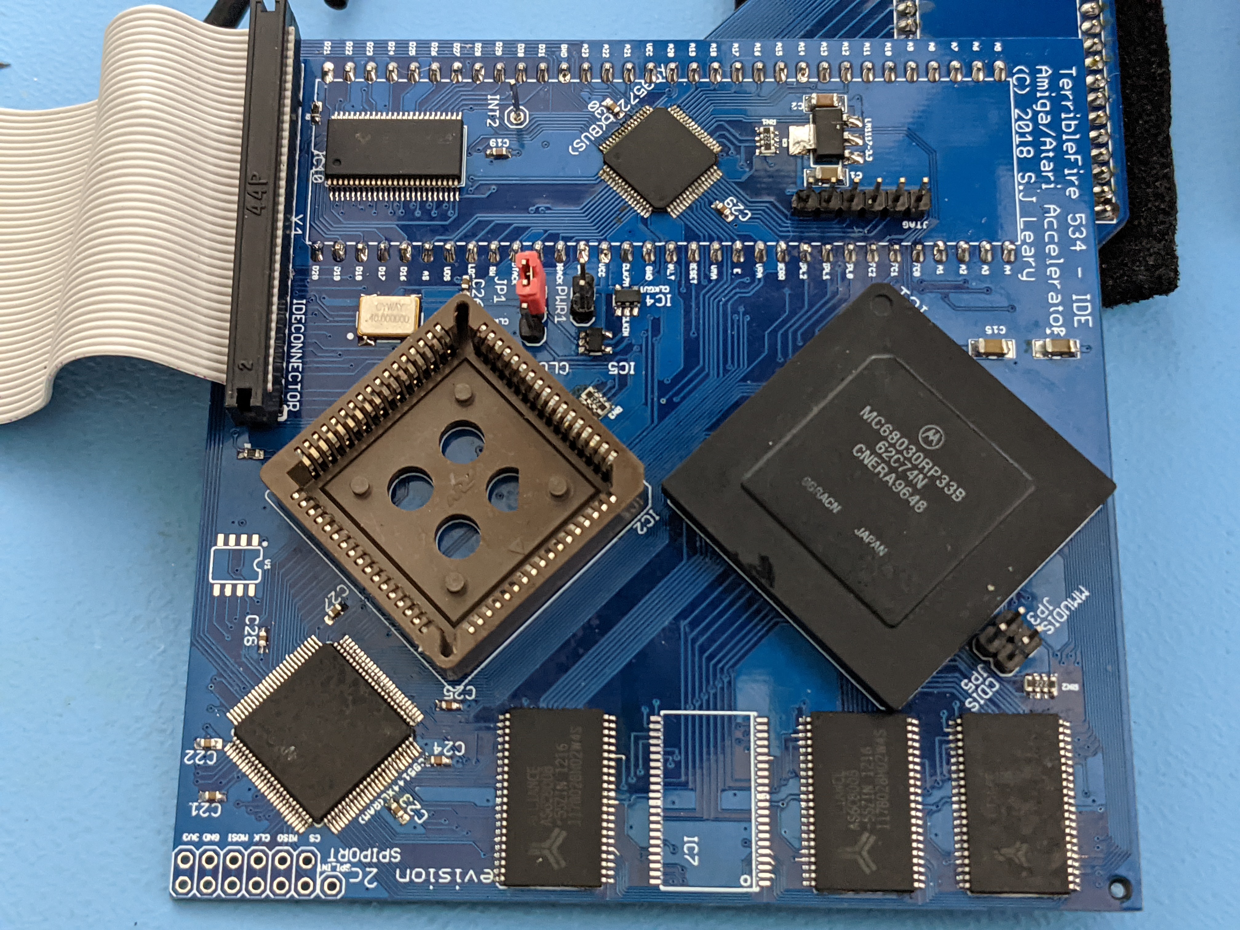
Now, “product 1” on this board is the RAM, which indicates the diagnostics on the RAM completely failed. So first of all I took a look at the board under a microscope. It is not the best made board I’ve seen. The list of problems I can see are:
- There appears to be a mix of types of solder
- The CPU is soldered directly to the board instead of socketed
- The pins on one of the CPLDs are bent
- There is flux all over the place
- Square pins were used at the bottom so it will not work on a regular relocator
This is all on top of the fact this is a HASL PCB which would have made the original soldering of the surface mount components a nightmare. HASL stands for Hot Air Solder Leveling, basically the board is dipped in molten solder to protect the copper underneath. The problem with this is you don’t get a very even finish. The alternative process is called ENIG which stands for Electroless Nickel Immersion Gold which is basically a gold plating of the board, this gives a visually nicer finish and is a much more perfect surface to solder onto. Unfortunately it is also significantly more expensive.

I saw a few potential flaws in the soldering and corrected those, but this didn’t correct it. I then ran a memory test in Amiga Test Kit using the manual address range of the RAM to see if it would find the flaw.

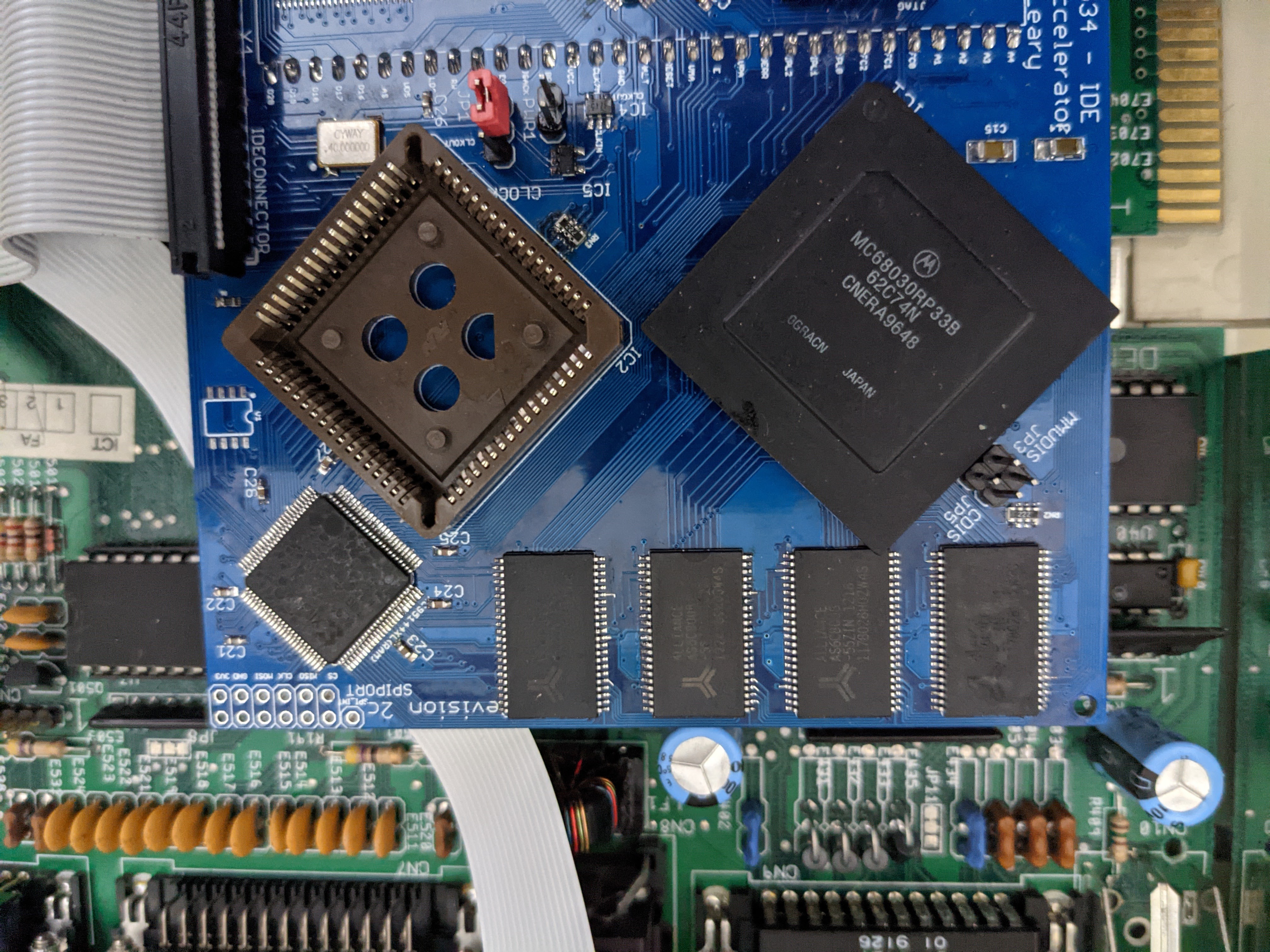
This is useful, the TF534 has 4x 8bit chips to make up a 32bit data bus (ignore the 16bit result). This clearly shows that one of them failed. I did a “finger test” to see if any of them were hot. I won’t be doing that again, I later used a laser thermometer and found that one of the chips was 80°C. Judging by the schematic for the TF534, IC7 provides D23-D16. IC7 was also the chip that was hot, so this is very likely a failed RAM chip.
IC7 is the second rectangular chip from the left at the bottom of the board. So, I protected the surrounding components with heat resistant polymide tape, I used some flux, added some low-temperature solder to all the pins, added some more flux and then used a hot air gun and tweezers to carefully remove the chip. Then to clean up I removed the remaining solder using a solder wick and cleaned the area with isopropyl alcohol. The prepared area then looked like this.
The next day the replacement RAM chip arrived. I soldered this on using my microscope, flux, 0.5mm solder and a 0.3mm tip (I need to get some thinner solder at some point). Again cleaned the area and put it into my test Amiga.
The machine booted without a diagnostic error and I managed to run Amiga Test Kit’s memory test without fault for a half hour or so before I declared this board good. Also no more burns to the finger when removing the board!
I have a new ultra-sonic cleaner coming so I’ll give this a good clean in the next few days and then return it to its original owner.


Leave a comment