There is a project called the RGBtoHDMI project which is quite popular at the moment. Put simply it a project that pushes raw digital RGB data into a Raspberry Pi Zero which then spits that out on its HDMI to produce a low-latency, pixel perfect representation of the image. It was originally designed for Acorn computers but there are now adaptors for various platforms.
Of course there are Amiga versions of this, a GitHub user called c0pperdragon created the first Amiga 500 version of this and Bloodmosher created an Amiga 2000 one. I then created an update version of this which I’m going to talk through in this post.
Theory of operation
Most versions of the RGBtoHDMI takes 6 and 8 bit RGB and sync data into a CPLD which works out the timings and then feeds the data into the Pi. The Amiga variants instead use logic gates and the Amiga’s only clocks to provide the pixel clock and directly pumps in the 12 bit colour data.
Amiga 500s and 2000s use a video chip called “Denise” and there are two possible variants OCS (Original Chip Set) and ECS (Enhanced Chip Set), the chip for latter also called “Super Denise”. Unfortunately the timings of these are slightly different, which will become important later.
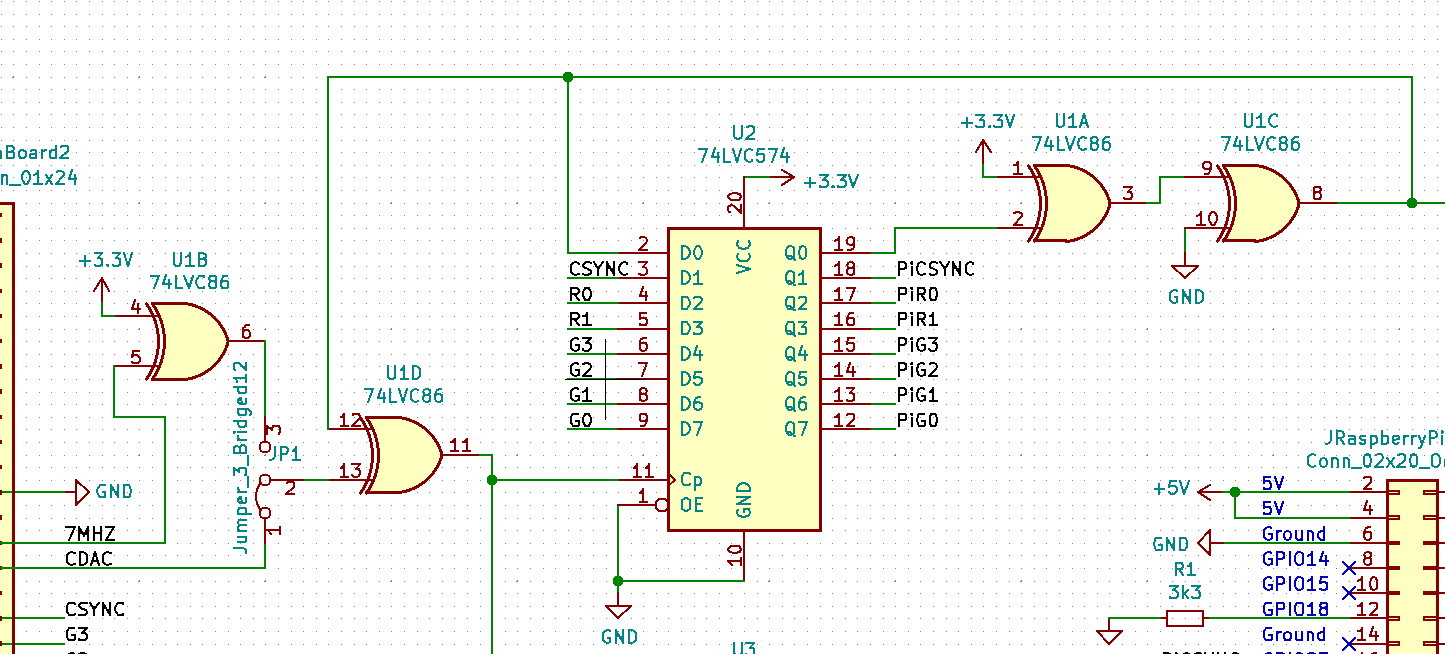
The pixel clock is 14Mhz and there are two different 7MHz clocks provided to the Denise chip. I won’t go into too much detail as to what is going on below (in part because it gives many people a headache), but basically it uses either the inverted 7MHz clock for Super Denise or the CDAC clock for Denise, uses the flop-flop to double to clock bandwidth to 14MHz and adds a small amount of intentional latency based on the calculated gate transition time.

This adaptor sits between Denise and its socket, capturing the signals, processing them in the gates and pumping them to the Pi. If the incorrect clock is used you can end up with a severe “sparkling” effect due to the RGB signals not always aligning with the clock used as a pixel clock.
Now, for the Amiga 2000… The Amiga 2000 and many big box Amigas actually have a video slot inside them which provides the digital RGB and sync signals. So it is possible to create a video slot version of this which is great because there is not much physical room to put the Amiga 500 version under an Amiga 2000’s Denise.
The only small issue is there is no 7MHz clock, but there is the CDAC clock and two other clocks (C1 and C3) which can be XNOR’d to produce the 7MHz clock.
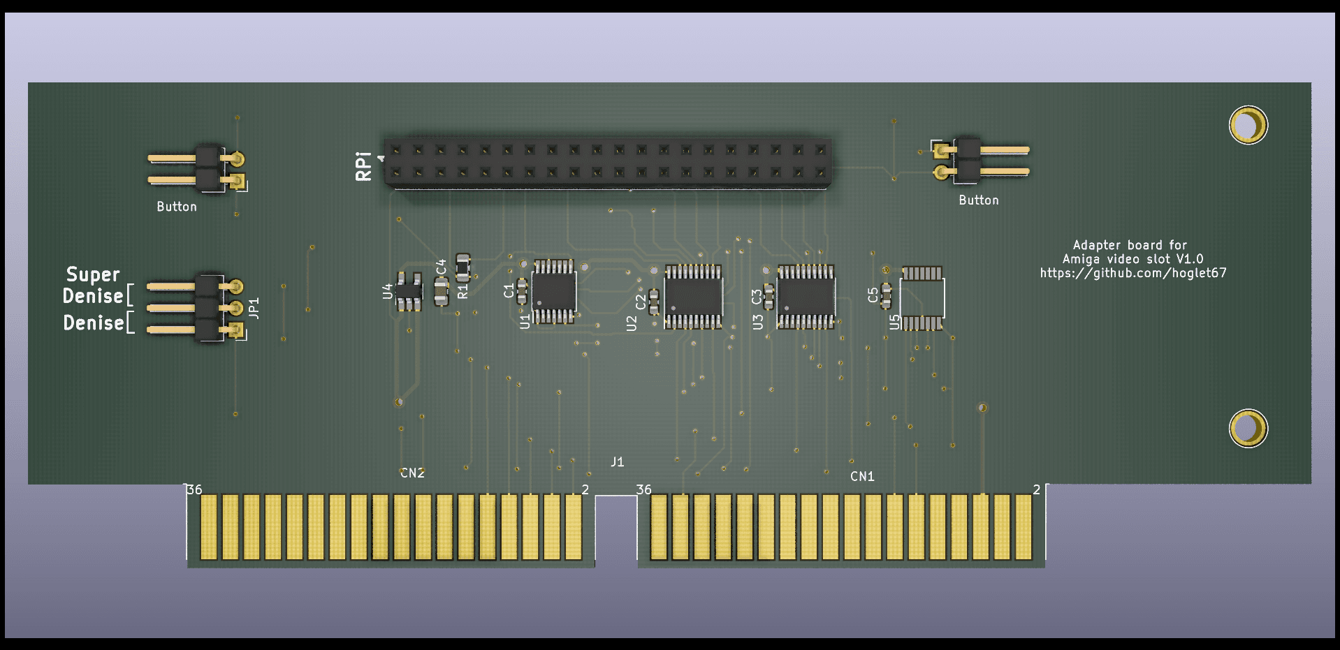
Bloodmosher’s build
Bloodmosher did an excellent job of creating the first Amiga 2000 version of this which can be seen below. He added U5 which does an XOR of the C1 and C3 clocks and then uses another XNOR as an inverter to turn this into a 7MHz clock. This is then inverted again in U1 to create the Super Denise clock. Apart from that it is functionally identical to the Amiga 500 version.

Unfortunately I’ve had several timing issues with this design and occasional other problems which have caused issues after several hours of continuous operation. Some of these were fixable by adding a tiny capacitor between the pixel clock and ground, some were fixable by using another IC with a slightly different gate latency. I decided to take another approach and redesign the board.
LinuxJedi’s build
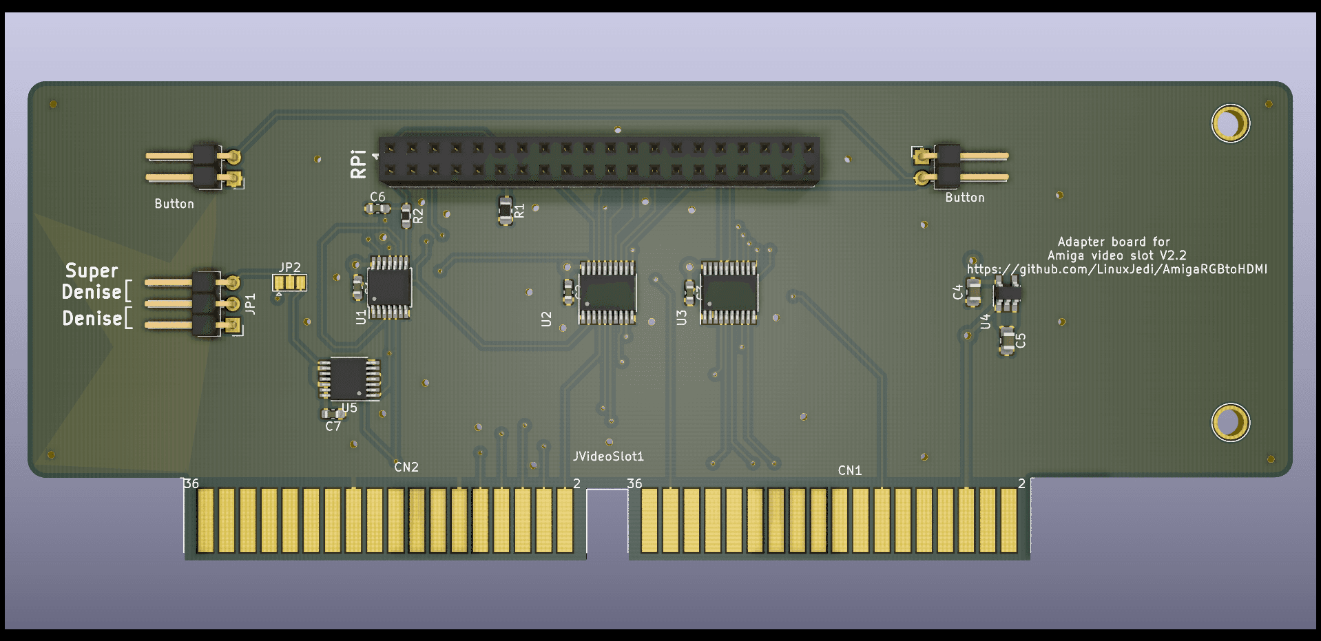
You can see below that my build is somewhat similar, but there are several changes particularly around attempting to improve stability and to give different timing options.

First of all I move the components to places closer to where their inputs and outputs are, avoiding tracks that are longer than are needed and reducing the amount they had to cross each other. I also manually routed the board instead of the autorouting in V1 which significantly reduced the number of signal vias.
Next up the options. In the V1 build the Super Denise clock was generated by doing C1 XOR C3 in U5 which is then inverted in U5 and then inverted again in U1. I figured this was introducing unnecessary latency. So, the first option in the board was to either just do C1 XOR C3 in U1 or do the original gate routing all in U5. You can switch between them by soldering the option required in JP2. This also makes U5 entirely optional.
There is also an optional RC delay in R2 and C6. Several people were finding that a 47pF capacitor between the pixel clock and ground was improving things. So a 0ohm in R2 and a 47pF in C6 on my design would give the same effect. Or you could just leave C6 completely unpopulated.
I also made a few general improvements that should help with stability:
- U5 in the original design had floating inputs which is bad for CMOS chips, unused inputs are now pulled high
- There is now a ground pour on both sides to help avoid stray capacitance
- There are more ground points for the Amiga and Pi
- The voltage regulator has an input capacitor which most datasheets recommend
Finally I rounded the edges of the board, just because I waned to.
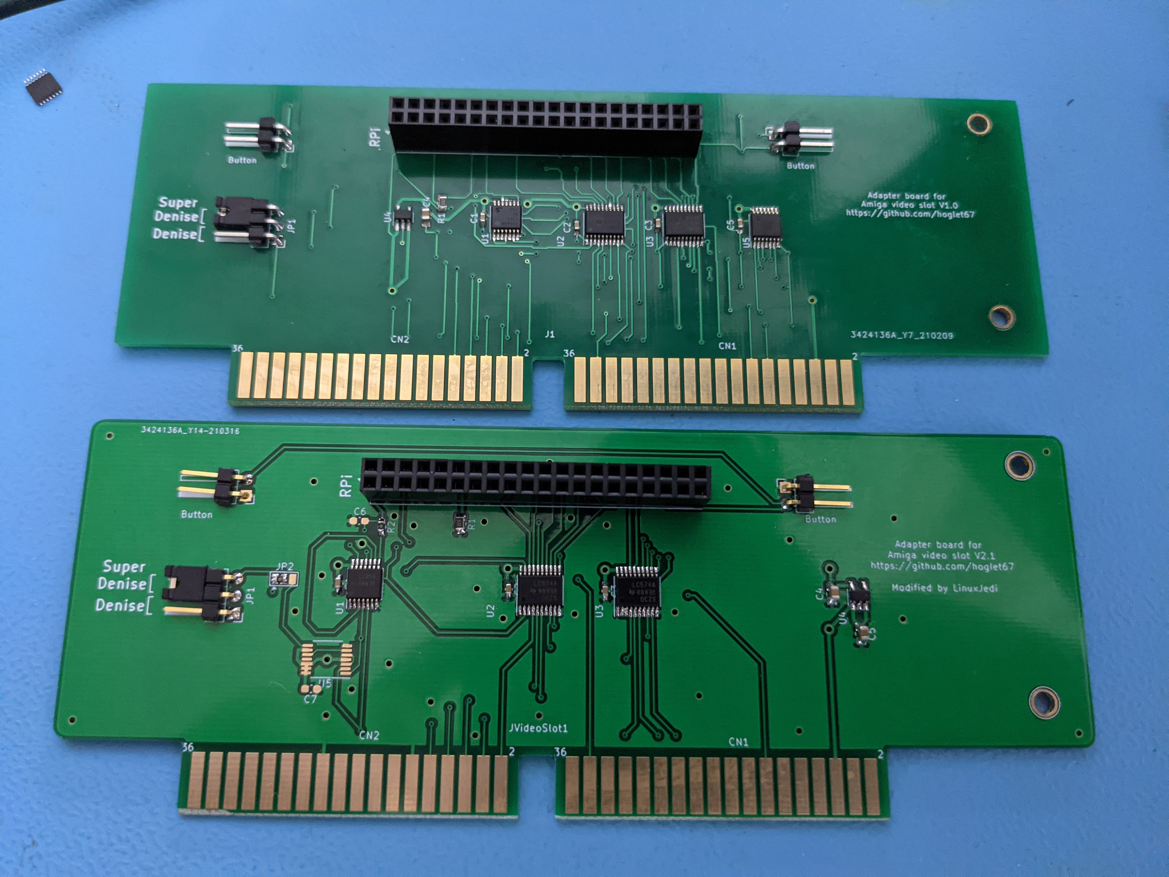
You can see in the image below the original V1 board at the top and my V2 board below set as the option without U5.

Conclusion
I’ve built a batch of these boards which have been sent to various people in the Amiga community and so far they have been stable (one minor colour issue to a soldering mistake I made). It appears at the very least that my changes do no harm and save a whole logic chip from being used. My design can be found on GitHub here.
I’m not stopping here though. I have ideas for even more improvements which I can hopefully share in the coming weeks.


Leave a Reply